
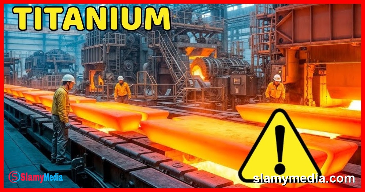
and Phi Mechanics in the domestic semiconductor ecosystem. Unlike European EUV systems, which are optimized for maximum compactness and precision, China's prototype adopts a brute force approach accepting a larger footprint and higher energy consumption to reach the same objective, generating a light source powerful enough to etch chips. And that is starkly evident in its design. This machine is not a single piece of equipment. It is an assembly of massive interconnected modules. The laser system is housed in its own section, the tin droplet generator and another, vacuum chambers, cooling systems, high capacity power supplies, stretching out like an industrial assembly line. The entire system's footprint was can occupy an entire factory floor, spanning hundreds of square meters many times larger than the packaged designs from the west, a single machine, but like a miniature factory. While a European EUV machine can be packaged into a size comparable to a 15 to 20 meter bus, China's prototype is more of an expansive industrial complex, where laser, cooling, power and control systems are decoupled and maximized to minimize instability risks during operation. At the core of the machine is the L, P, light source. Laser-produced plasma considered the heart of EUV technology, where ultra high power lasers strike molten tin droplets 50,000 times per second, creating plasma points at temperatures of approximately 200,000 degrees Celsius, emitting ultraviolet light with a 13.5 nanometer wavelength. Small enough to etch semiconductor circuits at the atomic level. But for this system to operate reliably, it needs more than just a heart. It requires a complex anatomy. Directly in front of the light source is an ultra high vacuum chamber, where the entire process occurs in a near-airless environment. Because a single dust molecule, or even a thin layer of gas is enough to completely absorb the EU of beam, an environment akin to deep space. Inside lies a multi-layer reflective mirror system, coated with dozens of atomic-scale layers of material, finished with near absolute smoothness to reflect EUV light instead of absorbing it. Because at this wavelength, conventional lenses are completely useless. Light does not pass through. It can only bounce. Each reflection loses energy. Therefore everything must be mathematically precise. Next is the wafer stage, a high precision mechanical system moving at extreme speeds, while maintaining nanometer level tolerances, where every minute movement is governed by laser sensors and algorithms. A single movement. But it must be thousands of times more accurate than a standard CNC machine. Running in parallels the control and synchronization system, where the entire process from laser firing and plasma generation to light reflection and wafer movement is calibrated in real time with near zero latency. One beat late, and everything is ruined. To sustain this state, the machine requires a massive cooling system. As the heat generated comes not just from the 200,000 degrees Celsius plasma, but from the high intensity lasers operating continuously, a colossal heat source that must be perpetually
controlled. Behind it all is the power supply system, where megawatts of electricity are stabilized to feed the entire machine, making it one of the most energy intensive devices in modern manufacturing. In essence, this system is performing something utterly absurd. It generates a light source that nature does not readily provide. A wavelength too small to remain stable. And then it bends that light through a series of multi-layer reflective mirrors with atomic level smoothness. Because at this wavelength, light cannot pass through ordinary lenses, but can only reflect in a near absolute vacuum, where a deviation of even a single nanometer can render the entire system ineffective. What this machine produces is not just light. It is the foundation of the entire modern digital world, an extreme process, not just in terms of energy, but in terms of precision. Because every laser strike must not only hit the correct position, but also occur at the exact time, with the exact intensity and hit the exact shape of the tin droplet, because the slightest deviation means the plasma will not form correctly, and the entire EUV light chain will collapse instantly. Imagine this. You are trying to use a gun to hit a drop of water smaller than the head of a pin, 50,000 times per second, while that target is in constant motion. And the entity controlling it all does whole our way, not in the way a tech company operates a product. But like the command center of a national scale campaign, where every resource, every person, and every problem is pulled toward a single point to solve an objective with virtually zero margin for error, not incremental development, but extreme acceleration. To understand how this model operates, well, Bubby Atni kicking, Baushapas, look back at the Manhattan Project, the United States top secret program during World War II, where over 130,000 people were mobilized to develop the atomic bomb using a specific structure, breaking everything down to the point where each group knew only its own task. Yet the entire system surged forward at an unprecedented pace, a fragmented system, but extremely efficient. And that is exactly what Huawei is replicating in the EU of race. They do not do it all themselves. Instead, they act as the coordinator, deconstructing complex problems from plasma light sources and reflective mirrors, to nano-controls, and assigning them to specialized groups for parallel processing before integrating them into a finished system. No one sees the full picture, yet the picture is completed. The entire project is organized under a compartmentalization model, meaning information is fragmented to the point where each group remains unaware of the broader scope, minimizing the risk of leaks and allowing different segments to be developed in parallel at maximum speed. Each person sees only a fragment. The system still operates seamlessly. In many cases, engineers work under aliases, use fake ID badges, face restricted intergroup communication, and even live on site during critical phases. Creating an environment almost entirely isolated from the outside world to maintain absolute
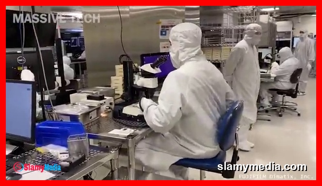
secrecy and focus. A laboratory, operating like a military unit. However, creating an EUV system is only 80% of the battle. The remaining 20% risk, the hardest part lies in materials and durability, where it's no longer about the theory or operating principles, but the ability to survive and operate stably in the most extreme environment humans have ever created. The remainder, that is what decides everything. The greatest challenge lies in the reflective mirror system. The optics where EUV light must bounce across dozens of ultra-flat surfaces with atomic level precision, because at a 13.5 nm wavelength, this light cannot pass through any conventional glass or lens. Impermeable, only reflection is possible. But the problem is these mirrors don't operate under normal conditions. They are subjected to the direct impact of plasma generated from molten tin at temperatures reaching approximately 200,000 degrees Celsius, causing their surfaces to continuously erode at a microscopic level. Even an infinitesimal degradation is enough to render the entire optical system ineffective, one slight deviation. Total loss of light. Currently, China has succeeded in manufacturing these multi-layer mirror systems, but the primary weakness isn't production capability. It's long-term durability. The reflective surfaces cannot yet maintain stable performance over extended operating cycles, forcing constant adjustment, replacement, and optimization during trial runs. Still unstable, yet operational. Parallel to this is a pragmatic strategy, procuring legacy lithography systems from the secondary market, from Nikon and Ancannon to older ASML models, then dismantling every component to analyze their design and discover how to replicate them using domestic technology. No shortcuts, but utilizing every possible data point. However, even if the material problem is solved, another challenge remains. The yield rate, generating EUV light is only the first step. Printing millions of chips with low error rates and at speed sufficient for commercial production is an entirely different equation. Not just precision, but precision repeated millions of times. This requires nearly perfect mechanical systems where the wafer stage must move with nanometer level tolerances while maintaining high speeds. All while the system controls thermal drift, because even the slightest thermal expansion of materials can misalign the entire chip printing process, a microscopic change, but a catastrophic consequence. This is why an almost immutable law exists in the semiconductor industry. You can achieve 80% of the technology in a relatively short time if you have sufficient resources, but the final 20% of the refinement, optimization and commercialization is where the most time and effort are consumed. Fast at the start, slow at the finish, from a practical standpoint, coin, China may have covered most of the ground in terms of principles and systems, but the remaining gap, the hardest

part, will likely stretch into the 2028-2030 period when every element from materials and mechanics to controls must reach near absolute perfection. And that is the ultimate test, not creating the technology, but making it survive in the real world. EUV marks a strategic turning point for China, not merely in technology, but in its standing within the global economic and power hierarchy, as they gain the opportunity for the first time to control one of the most fundamental technologies of the 21st century. A new gateway, and behind it lies the entire future. For China, the paramount value of EUV lies in the capacity for total autonomy in advanced semiconductor manufacturing. This signifies the ability to develop AI, high performance computing and military systems without reliance on foreign licensing or external supply chains. No longer obstructed, no longer delayed, amidst increasingly stringent technological restrictions, possessing domestic EUV is akin to eliminating the single greatest vulnerability in the entire industrial framework, as bottlenecks once controlled by external forces are replaced by internal development capabilities. A choke point has vanished. Once that bottleneck ceases to exist, the developmental velocity of the entire technology sector from chip design firms and equipment manufacturers to the AI ecosystem may be unleashed, triggering a growth cycle previously constrained by factors beyond their control, an ecosystem accelerating in unison. Yet the impact of EUV does not stop at China's borders. It radiates globally. For decades, the semiconductor industry has operated as a centralized structure, where core technologies were held by a select few nations and corporations, creating a relatively stable balance of power, an established order. An EUV has the potential to shatter it. Should China truly master this technology, the world will no longer rely on a single source for advanced chip manufacturing systems. A new center of gravity will emerge, forcing shifts in supply chains, pricing, and the technological strategies of other nations. A new poll in an old game. This could lead to a more comprehensive state of competition, where nations are compelled to accelerate investment, drive technological innovation, and reconstruct their own supply chains to avoid obsolescence. A new race, faster, more intense. From an economic standpoint, the emergence of a new EUV ecosystem could drive down semi-conductor production costs in the long term as competition intensifies in production scales up. Controlling growth across a multitude of industries dependent on semiconductors, from consumer electronics to electric vehicles and AI, costs decline, technology proliferates. Conversely, it raises profound questions regarding the fragmentation of the global supply chain, as technological blocks may gradually decouple, creating isolated ecosystems rather than

the unified system that previously existed. And that is the most dramatic part of the story. For years, the United States dominance has not rested on manufacturing everything itself, but on its ability to control the irreplaceable links in the global value chain, from chip design and EDA software to AI of P.Y.S. And the geopolitical leverage over the Netherlands in Japan to block advanced semiconductor equipment from flowing into China. Meanwhile, the Netherlands through ASML holds the most critical technological valve as commercial EUV remains the near absolute domain of the single company. But if China overcomes that specific link, the entire power structure begins to reverse. Because at that point, hardware bands will no longer provide the same level of leverage as before. What was once locked from the outside will gradually be opened from within. This is why Reuters sources describe the EUV project in Shenzhen as a leap that could undermine the West's most vital containment tool, even while the prototype remains in the testing phase and has yet to produce commercial chips. From a broader perspective, what the US fears is not just a single machine, but China's progress toward an end-to-end semiconductor supply chain. This means controlling more and more links from equipment and materials about to foundry capacity and finished chips. In fact, China has become the world's largest investor in chip making equipment in 2025, according to SEMI. And domestic wafer capacity continues to surge. If that scenario takes shape, the Netherlands will find itself in a very difficult position. ASML is not just a tech company, it is a European strategic asset. Yet the Dutch government has repeatedly had to balance security pressure from the US against its own economic interest with China, a market that remains critically important for ASML survival. For the global technological map, the greatest consequence may not be the US losing everything overnight, but rather the center of the AI and advanced computing race shifting from a West controlled system to a world with a new technological poll in East Asia. There, Shen Zeng, Shanghai and China's semiconductor industrial clusters will no longer be mere factories, but centers that establish the new rules of the game. And if that happens, the question will no longer be whether the West can stop China. But how will they adapt when the final barrier is no longer an absolute one? The semiconductor race has never been just about chips. It is about who controls the future of technology. And if EUV is truly mastered for the first time in decades, the global balance of power could begin to shift. A boundary has just been shattered, and the world will never be the same again. So in your view, if the final bottleneck truly vanishes, who will define the next era of AI the United States or China? Leave your thoughts in the comments below and don't forget to subscribe to Massive Tech to keep pace with the technology's reshaping our world.

Conversations (0)
Please log in to join the conversation.